
Dentists - Doctors - Inventors - Medicine - Science
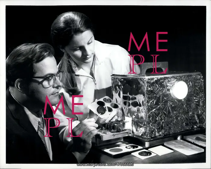
Dec. 12, 1972 - For A.M. Release, Tuesday, December 12, 1972: A unique process that uses intense ultraviolet light to speed and simplify the fabrication of semiconductor wafers has been invented by scientists at the General Electric Research and Development Center, Schenectady, N.Y. The process uses ultraviolet irradiation to clean excess photoresist from semiconductor wafers - a long-standing problem in the semiconductor processing industry. Dr. Donald A. bolon, developer of the technique, and Mrs. Karen K. Webb, a technician, prepare to run sample wafers through a test chamber. The process is the first that lends itself to the continuous and dry removal of excess photoresist materia, a plastic film used in etching microscopic circuit patterns onto semiconductor wafers
Pick your License
Restrictions Only for United Kingdom
Circuit Clean Continuous Developer Excess Fabrication Intense Invented Irradiation Itself Lends Long-standing Materia Microscopic Onto Prepare Processing Removal Schenectady Scientists Semiconductor Simplify Technician Tuesday Ultraviolet Uses Wafers
Features In These Collections
> Contributors > KEY


